Andreas Frölich, CEO, Horizon Microtechnologies
Horizon Microtechnologies is a company expert in coating processes that add material and functionality to a microstructure, all developed to work with a range of materials and shapes. Effectively, the company produces parts using the initial microstructure as a template, with its coating technologies making the final parts much more functional than the original template in a variety of ways.
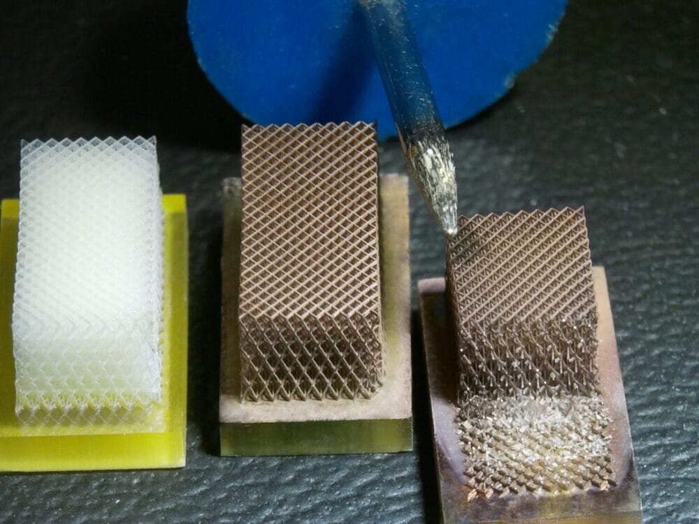
The technologies are especially suited as a post-printing treatment for micro-AM derived templates, and recently Horizon announced that is able to add copper metal coatings to polymer micro-AM and other micro structures. This means that for the first time, companies can produce parts with the functionality of copper but also exploit the design freedom, precision and resolution achievable through micro-AM.
The ability to metallically coat micro parts in metal (or to fabricate them directly in metal) is not new in itself, and a number of process options exist. This article will benchmark these different metal fabrication processes, and compare them with the newly launched metal coating technology commercialized by Horizon.
In particular, we will look at coating technologies (including metal Atomic Layer Deposition (ALD), Chemical Vapor Deposition (CVD), physical vapour deposition (PVD) or sputtering), electroless plating and electroplating, and direct fabrication processes including metal 3D printing, and metal injection moulding (MIM). We will not consider spray- or dip-coating since these approaches usually aren’t precise enough to be useful for micrometer-scale parts or parts toleranced on the micron-scale. Also, we will exclude direct-write approaches such as ink-jet deposition.
NOVATEK CAMERA
Making Metallic Objects
Companies may choose to apply metal coatings to polymer microstructures instead of manufacturing metal parts for several reasons. Firstly, given a suitable process, coating microstructures with metal allows for precise and controlled deposition of the desired material on the desired areas, enabling the post-production modification of the microstructure with almost no change to its dimensions and without needing to adapt the microfabrication process. Hence, this approach offers additional flexibility and opens up customization options.
Additionally, coating microstructures with metal can be more cost-effective than bulk metal micromachining, as it minimizes material waste and reduces production time compared to traditional metal part manufacturing. Furthermore, metal coatings provide opportunities for improving functionality by enhancing surface properties such as conductivity, corrosion resistance, and wear resistance. By applying metal coatings to microstructures, companies can achieve desired performance characteristics while maintaining the bulk properties of the original substrate material such as (in the case of polymer) lower density, and higher flexibility.
A number of alternative metal coating technologies exist, each with pros and cons.
Atomic Layer Deposition. Atomic Layer Deposition (ALD) is a precise thin film deposition technique used for coating surfaces with a variety of different film materials. In the ALD process, two or more precursor gases are alternately introduced into a vacuum chamber. The precursors react with the substrate surface in a self-limiting manner, forming a monolayer of metal atoms. Each cycle of precursor exposure and purging deposits a single atomic layer, allowing for precise control over the film thickness. The process continues until the desired film thickness is achieved.
While ALD has good conformal coating capabilities, even on complex three-dimensional structures, there are some disadvantages to consider. ALD is a slow and time-consuming process due to the requirement for sequential precursor exposures and purging steps, and the deposition rate is relatively low compared to other techniques. While in theory thick ALD films can be grown, 200 nm or less are often considered the practical thickness limit. Furthermore, not all film materials can be grown on all substrates and temperatures of 100° C or higher are often needed. The equipment and setup for ALD are typically costly and complex, and certain precursors used in ALD may be expensive, dangerous or toxic, requiring careful handling and disposal procedures. Additionally, metals are the most challenging materials to deposit by an ALD process.
Chemical Vapour Deposition. Chemical Vapour Deposition (CVD) is a widely used process for depositing metal and other films onto substrates. In a metal CVD process, a metal precursor gas, often along with a reactive gas, is introduced into a vacuum chamber containing the substrate which often must be heated to 200°C or higher, depending mostly on the precursors used. The precursor undergoes chemical reactions at the substrate surface, resulting in the deposition of a metal film.
With the right process conditions and precursors, CVD can achieve deposition of good quality, conformal metal films on various substrate shapes and sizes, including complex and three-dimensional structures, but the process typically requires high temperatures to facilitate the chemical reactions, which may limit its application to certain temperature-sensitive substrates. As with ALD, the equipment and setup for CVD can be complex and expensive and many precursors are hazardous, toxic, and difficult to handle.
Physical Vapour Deposition/Sputtering. Physical Vapour Deposition (PVD) and sputtering are techniques that involves the vaporization of a metal source and subsequent condensation onto a substrate. In these processes, metal atoms are released from a metal source inside a vacuum chamber either by heating or ion bombardment. The metal vapour then travels and condenses onto the substrate surface, forming a thin film. The deposited material is the same as the source material with no chemical reaction taking place between evaporation and condensation on the substrate (in contrast to ALD and CVD), and the deposited film is in principle as pure as the target material.
Also, PVD can often be conducted at relatively low temperatures, minimizing the risk of substrate damage or distortion.
However, PVD is limited to (nearly) line-of-sight deposition, meaning that it has challenges in coating complex three-dimensional structures, e.g. with undercuts or overhangs. Additionally, PVD equipment can be expensive and require specialized knowledge for operation and maintenance.
Electroless Plating. Electroless plating is a metal deposition process that occurs without the need for an external electrical current. In the electroless plating process, a substrate is immersed in a solution containing metal ions and a reducing agent. The reducing agent initiates a chemical reaction, causing the metal ions to be reduced and deposited onto the substrate surface. The process is self-sustaining and continues until the desired thickness is achieved.
Electroless plating enables the deposition of uniform and conformal metal coatings on complex shapes, including internal surfaces and recessed areas, but the process requires careful control of the solution’s local composition, pH, and temperature to ensure optimal and consistent plating conditions. Electroless plating typically has a slower deposition rate compared to other methods, and the need for post-treatment steps, such as rinsing and drying, can increase processing time and complexity.
Electroplating. Electroplating is a commonly used process depositing a layer of metal onto a substrate from an electrolyte bath. It involves immersing the substrate, which needs to be conductive or at least have a conductive surface, in an electrolyte solution containing metal ions of the desired coating material. A direct current (DC) power source is used to create an electric field between the substrate and a counterelectrode in the plating bath, causing the metal ions to migrate to the substrate’s surface and form a thin, adherent metal layer.
One advantage of electroplating is its ability to coat intricate and delicate structures with high precision. The process can uniformly deposit metal also onto complex geometries and can reach “around the part” leading to simultaneous coating of all part surfaces, including recesses and hard-to-reach areas to some degree.
However, electroplating also has some disadvantages in the context of complex metal micro part fabrication. One limitation is the formation of edge build-up or uneven thickness distribution during the coating process, especially in sharp corners or high-aspect-ratio features. This can lead to challenges in achieving precise dimensions and can affect the overall quality and functionality of the micro parts. Additionally, the process typically requires multiple steps, including surface preparation and post-treatment, which can increase production time and complexity.
Direct 3D Printing. While advancements are being made in metal 3D printing, it currently faces challenges in terms of cost, material availability, and resolution that limit its commercial viability for micro parts compared to plastic 3D printing.
One key limitation is the achievable resolution and precision of micro metal 3D printing technologies, which may not be sufficient to meet the stringent requirements of micro metal parts. The layer-by-layer deposition process and the size of the metal powder used in 3D printing can result in rough surface finishes and lower dimensional accuracy, which can be critical in micro-scale applications. In comparison to photopolymer 3D printing, post-processing steps such as removal of support structures and sintering (which is typically required) introduce additional work and challenges to dimensional accuracy. Additionally, the complexity and cost of 3D printing equipment suitable for high-resolution metal parts can be prohibitive.
Coating processes for microstructures allow for customization, improved functionality, and preservation of some of the original microstructure material properties such as the light weight of polymer. Therefore, metal coating methods are often a more viable option for creating micro metal parts than direct 3D printing if bulk metal parts aren’t strictly required.
Metal Injection Moulding. Metal injection moulding (MIM) is often not as viable an option for producing micro and precise metal parts as metal coating due to several reasons. MIM is limited by the achievable resolution and complexity of the moulded parts which will always need to present a parting line/plane. The process relies on injecting metal powder combined with a binder into a mould, which may result in challenges when replicating intricate microstructures or achieving high precision. The resultant green parts are typically brittle which complicates ejection of micro-parts from the MIM tool. Additionally, MIM involves multiple steps, including debinding and sintering, which can introduce dimensional changes, affecting the precision of the final part.
Next Generation Metal Coating Technology
All the processes in the preceding comparison of metal coating technologies become challenging when working with complex, three-dimensional microparts. Achieving consistent deposition on all part surfaces requires precise control over process parameters such as flow rates throughout the part or line-of-sight to the surfaces . Obviously, this can be particularly challenging when working with complex part geometries, and is an area where Horizon’s research and development has been consistently placed.
Horizon has focused its initial efforts on copper metal coatings, as this opens up an array of application possibilities for companies wishing to add functionality to 3D microstructures and especially polymer micro-AM templates. Copper coatings can offer significant benefits for microstructures or micro-additive manufactured parts, but there are several challenges and problems associated with current coating solutions that Horizon has sought to address to ensure the successful application of the copper.
The company has carefully optimized the coating process, materials, and deposition parameters, and has largely overcome these challenges to harness the full potential of copper coating which can now be applied reliably, cost-effectively, and speedily, making it viable for a large range of applications.
Horizon’s copper coatings are typically in the 1-2 micron thickness range and reach conductivities between 10 and 16 MS/m, which is sufficient for many applications. Depending on the part geometry and a process-friendly part design, these values can be exceeded. Importantly, the company’s process can also coat internal channels and undercuts to some degree, the channel’s aspect ratio being the limiting factor now rather than the absolute length.
The technology is ideally suited to the very many applications where the use of bulk copper is not required and would be technically impossible or uneconomic. Making geometries via polymer AM not possible through the use of bulk copper, and then adding the functionality of a copper coating can therefore be highly disruptive.
Through Horizon’s metal coating technology, industry now has an alternative option when seeking to reliably coat three-dimensional micro-AM and other microfabricated objects with copper in a cost-effective and time-sensitive fashion.
The most important use case for the coatings is when highly conductive surfaces are required. Horizon’s copper coating can be used not just to coat an entire micro-part, but also allow to selectively coat or mask features on a part’s surface, creating several independent metal features for interconnects, vias, etc.
Copper coatings can also significantly improve the surface properties of micro fabricated parts by adding wear resistance, lubricity, and hardness.
The key application areas for copper coated micro-AM and microfabricated objects are those that require high precision, complex geometries, and advanced materials properties, such as high electrical conductivity. As such, opportunities exist in the production of micro-electronic devices such as free-form printed circuit boards, interposers and interconnects; micro-sensors; miniaturized biomedical devices (such as implantable sensors); drug delivery systems; lab-on-a-chip systems, micro-reactors, and microfluidic sensors; and MEMS actuators and transducers. Also, and importantly, mm-wave and RF components can be made using this approach which opens up the full design freedom of AM to RF-Designers. The additional degrees of freedom this offers are readily taken up by the antenna design community and have sparked a near-revolution in terms of new designs which optimize different performance parameters or greatly simplify the integration and assembly processes.
SUMMARY
This article has explored the various micro metal fabrication and coating technologies, and has assessed their pros and cons. Horizon Microtechnologies’ new copper coating technology for polymer microstructures emerges as a promising alternative. It offers precise and uniform copper coatings on complex micro parts, addressing the limitations of many alternative processes. With improved control over thickness and simplified processing steps, Horizon Microtechnologies’ innovation has the potential to disrupt the area of micro metal part fabrication, providing manufacturers with efficient and high-quality solutions for their needs.

